The Zeiss ORION NanoFab is an advanced scanning ion microscope that utilises an interchangeable dual-ion beam (helium and neon) for nanofabrication and sub-nanometre imaging
Imaging
The HIM excels at imaging surfaces with sub-nanometer resolution and high surface sensitivity. Imaging is achieved by detecting secondary electrons generated when the ions impact the sample surface. It offers new insight from materials with greater depth of field and can probe non-conductive samples without the need for coating. The NanoFab is thus well suited to imaging challenging samples such as polymers, nanoparticles and biological samples.
Milling / Deposition / Implantation
The HIM also offers unique nanofabrication capabilities. The Ne+ beam can be used for micro-nano milling, after which features can be refined using the He+ beam. Complex patterns can be generated using the Nanopatterning and Visualization Engine (NPVE) interface. A gas injection system (GIS) enables gas-assisted etching of silicon as well as ion-beam-induced deposition of tungsten and silicon dioxide. Nanoscale implantation studies using both beams can also be performed.
Specifications
- He+ beam (GFIS): 10 to 30 kV, Ne+ beam (GFIS): 10 to 25 kV
- Everhart-Thornley (ET) secondary electron detector
- Stage travel: x=50mm, y=50mm, z=8 mm, rotation 0-360°, tilt 0-56°
- Oxford Instruments OmniGIS II gas injection system: W, SiO2, XeF2
- Patterning Software: NPVE, 16 bit scan generator, create a range of fully editable shapes (array builder), full control over dose variation, real time image visualization
- Sample types: conductive, insulating, magnetic, hard and soft materials
- Limitations: High vacuum atmosphere. Escape of trapped helium can present a challenge in a few materials (notably silicon and diamond). Damage is generally low, but needs to be monitored
Sample Preparation
As with all vacuum techniques cleanliness is key. Samples should be free from moisture and oils, adhered onto a substrate or to double-sided conductive adhesive tape. Mounting on SEM pin stubs is preferable, please discuss with the instrument manager if you are not sure.
Access
The NanoFab can be operated by researchers or on a fee for service basis by MCFP platform staff. Trained users can book through the MCFP iLab booking system. Please note that training will only be offered to researchers for whom the HIM will form a large part of their research program, or where the user already has EM expertise. Please contact Anders Barlow to arrange access or training.
Additional resources
-
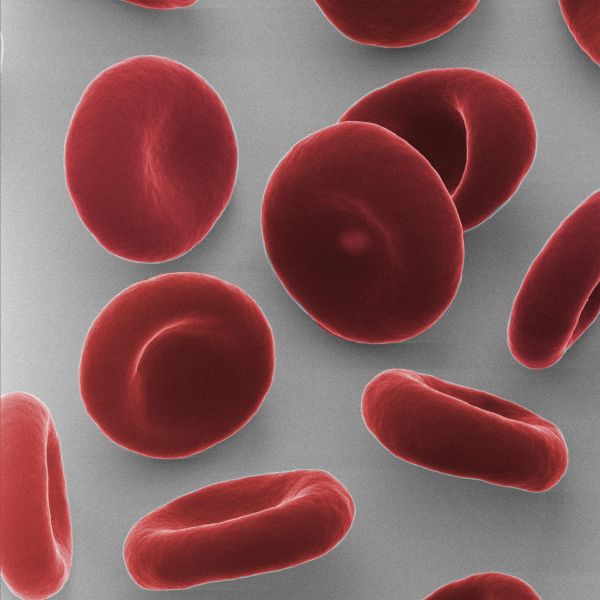
Red blood cells
Red blood cells -
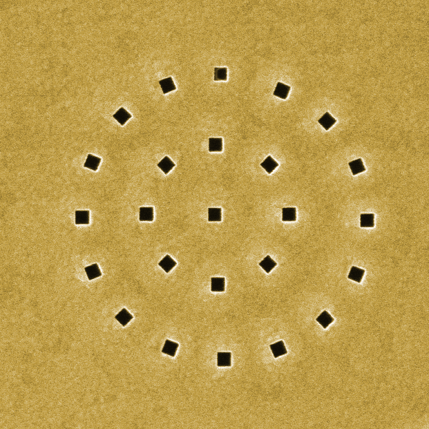
Nanoapertures in gold
100nm apertures milled into gold film on glass -
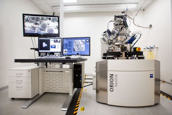
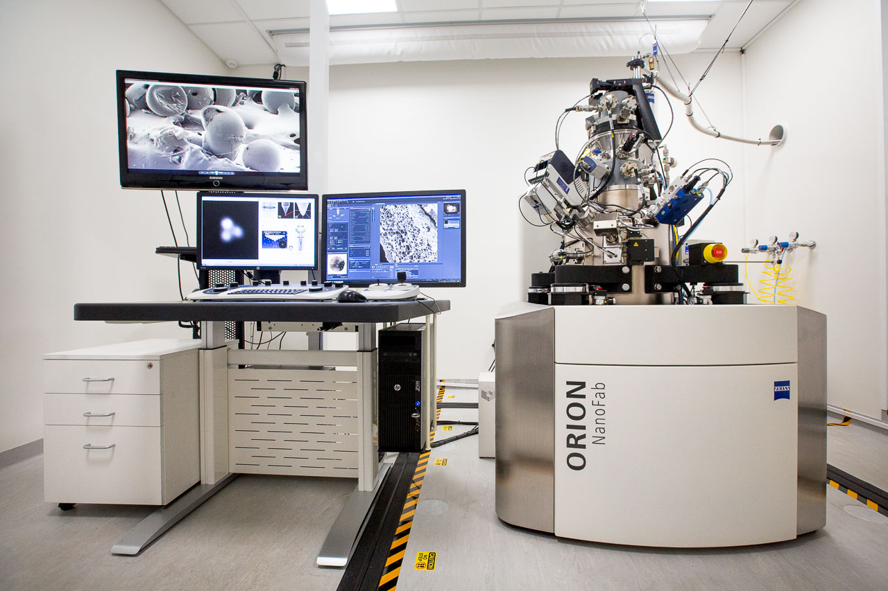
Zeiss ORION NanoFab
The Zeiss ORION NanoFab helium ion microscope (HIM) -
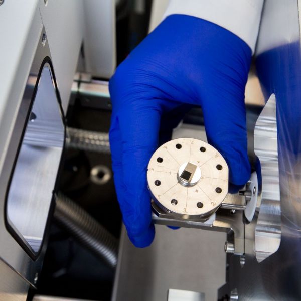
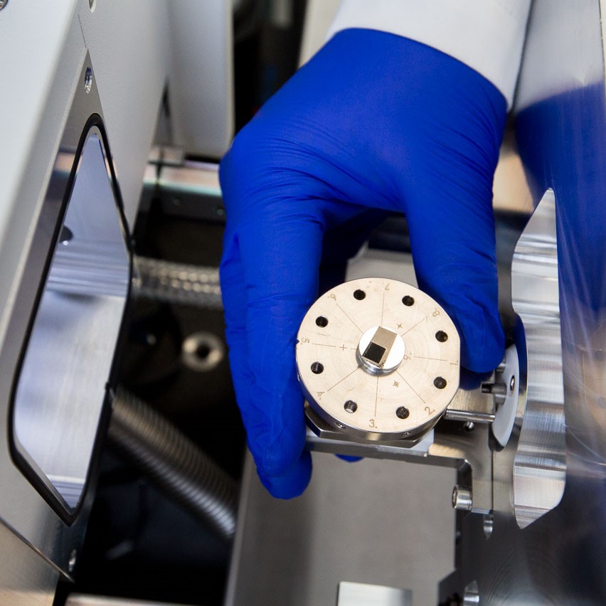
Sample stage
Standard pin mount sample stage for nine 12mm pin stubs -

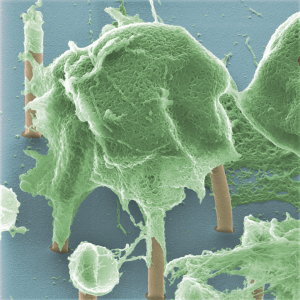
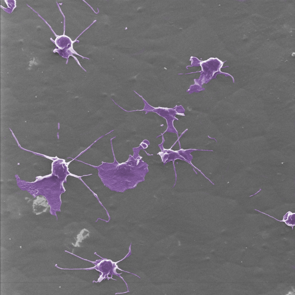
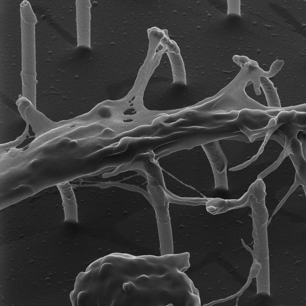
Cells on nanowires
Cells on vertical nanowires -
Cells on nanowires
Cells on vertically aligned nanowires -
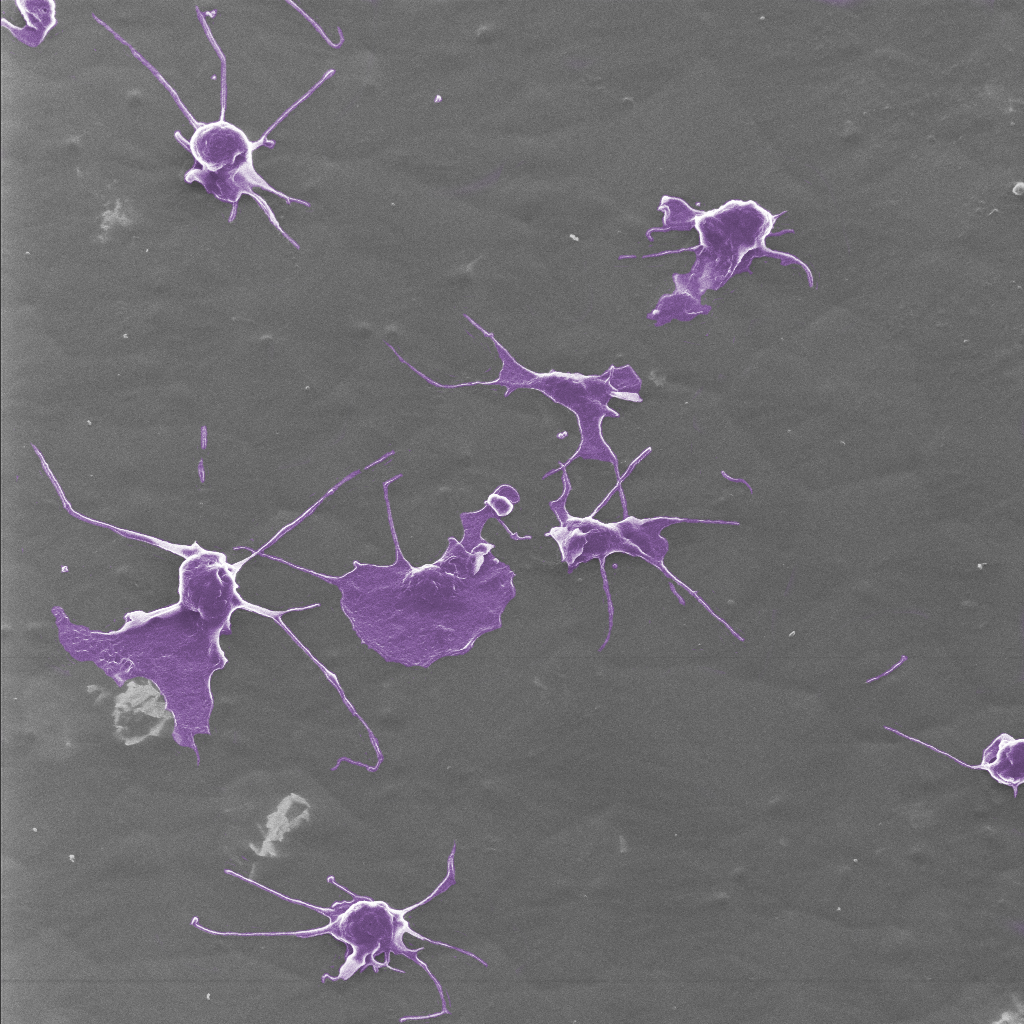
Cells on polymer
Cells on polymer film -
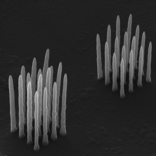
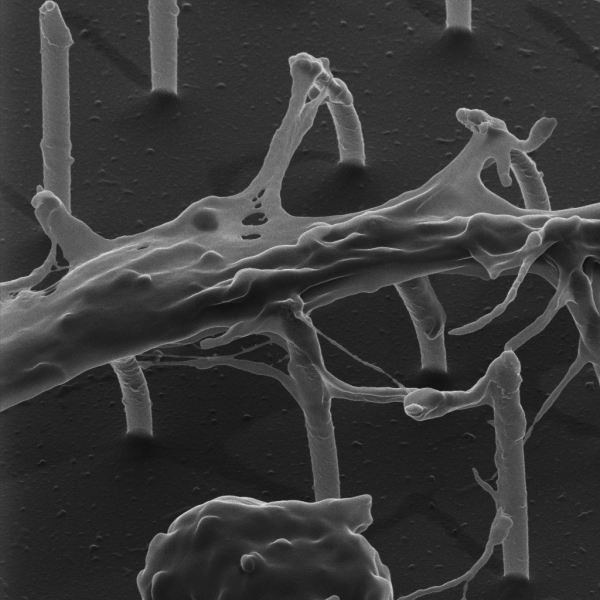
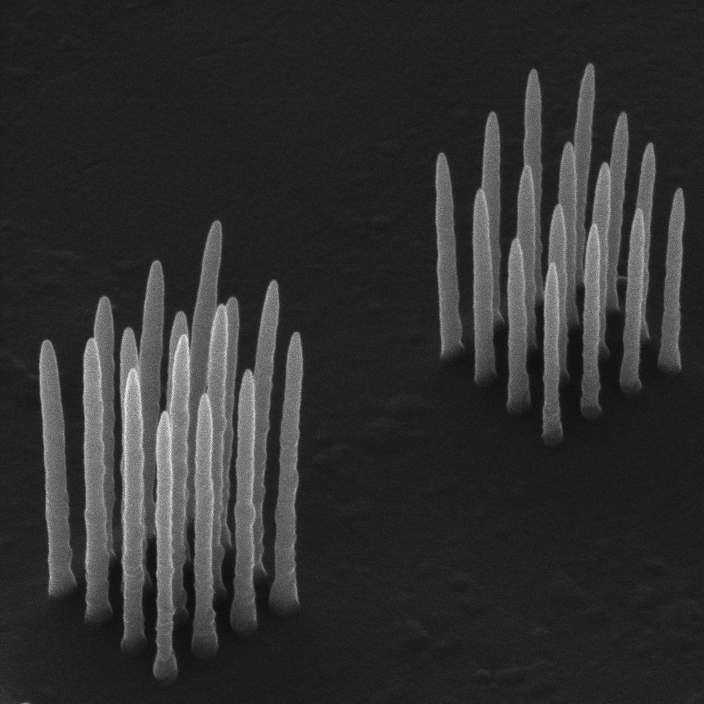
Vertical nanowires
Vertical nanowires by gas phase deposition


See Also
-
Scanning electron microscopy (SEM)
The FlexSEM 1000 is a rapid and easy to use variable pressure SEM amenable to imaging both conductive and insulating specimens
-
Hirox RH-2000 2D/3D microscope
High resolution imaging (HD/HDRI) and video recording (RGB/BW)
-
Confocal Raman Microspectroscopy
The Renishaw inVia Qontor confocal Raman microscope is capable of spectroscopy, mapping and live focus/topography tracking
-
Sample Preparation
We have flexible sample preparation capability for electron and ion microscopy including drying, ion polishing and sputter coating