High resolution (sub-nanometre) imaging, viscoelasticity mapping, electrical properties
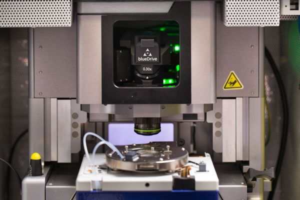
Cypher ES is a small sample AFM/SPM with striking ease of use.
Specifications
- Maximum image area x/y: 30 µm, z: 5 µm.
- Maximum sample size: 1.5 cm x 1.5 cm (if your sample is bigger please contact us to discuss about it)
- Resolution: 0.6 Å in the X and Y directions and 0.5 Å in the Z direction
- Manufacturer: Asylum Research/Oxford Instruments
Choose this instrument for:
- Closed loop imaging from tens of microns down to atomic scales
- Small cantilevers for high-speed scanning
- High-speed, low-noise force measurements
- High-bandwidth data acquisition
- Diffraction-limited optical sample viewing/imaging
- Automated laser alignment
Access
We can train you to do your own work, collaborate or do consulting work (fee for service).
For trained users, the Cypher is available on the MCFP's iLab Booking System. The instrument is booked per session.
- Morning session: 8am-1pm
- Afternoon session: 1pm-6pm
Sample preparation
In the process of sample preparation for AFM it is very important to minimise dust and contamination.
Our facility has a specific area for samples preparation, with two laminar flow cabinets, and all materials required.
For further advise on sample preparation please contact Tian below.

Tian Zheng
Academic Specialist - Nanomaterials Characterisation
Tian leads the nanomaterials characterisation (NMC) node of the MCFP. She can provide insight into all modes of modern atomic force microscopy measurements on a range of samples from nanomaterials to biological structures.
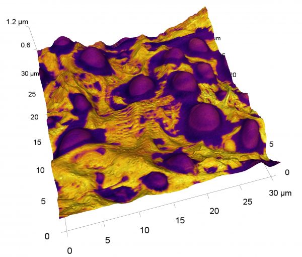
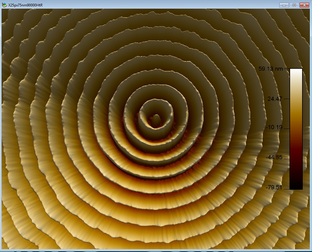
AFM Image Gallery
-
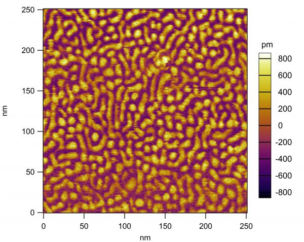
Topography of CTAB Micelles on Silica Sample provided by JJ Imaged on Cypher S AFM -
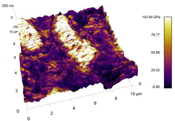
Elastic Modulus and Topography of Geopolymer Concrete Sample courtesy of Dr. Rackel San Nicolas Image taken on Cypher S AFM -
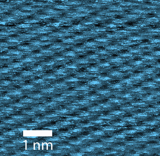
Atomic Resolution of Calcite in H2O Sample provided by Dr Cathy Sutton Imaged on Cypher S AFM -
Topography and Phase of Block Copolymer P2VP-PDMS Sample provided by Chao Chen Image captured by Cypher S AFM -
Topography of nanochannels produced on the NanoFrazor Explore Syetem Sample provided by Dr Srinivas Mettu Imaged on Cypher S AFM -
Piezoresponse force microscopy (PFM) lithography of PVDF film


See Also
-
MFP-3D AFM
High resolution imaging of large samples in multiple scanning probe microscopy modes
-
Hirox RH-2000 2D/3D microscope
High resolution imaging (HD/HDRI) and video recording (RGB/BW)
-
Scanning electron microscopy (SEM)
The FlexSEM 1000 is a rapid and easy to use variable pressure SEM amenable to imaging both conductive and insulating specimens