  1. Materials Characterisation and Fabrication Platform
  2. MCFP Learning
  3. Atomic Force Microscopy
  4. Fundamentals of AFM
  • Atomic Force Microscopy
  • Introduction
  • Applications of AFM
  • Fundamentals of AFM
  • Getting good images
  • Get into the lab!

Fundamentals of AFM

Video credit Oxford Asylum Research

Fundamentals of AFM

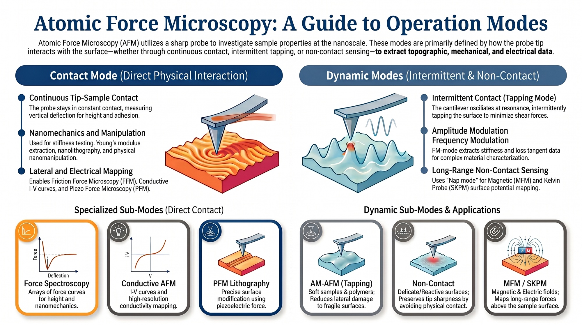
Depending on the type of interaction between the probe and the sample, AFM can be operated in multiple modes

Static Modes Dynamic Modes Electrical/Lift Modes

Static modes are sometimes also called contact modes, and include lateral force microscopy (LFM). They track constant deflection across the photodiode quadrants.

These can have various names including AC/AM/AFM, and track changes in peak-to-peak amplitude of oscillation and phase lag relative to the drive frequency/set phase.
(see embedded video below)

Conductive AFM (CAFM), scanning Kelvin probe microscopy (SKPM) and Magnetic force microscopy (MFM) modes require specialized conductive probes (CAFM and SKPM) or magnetic probes (MFM), and dual-pass scanning configurations (SKPM and MFM) to isolate electrical potentials/magnetic fields from underlying topography.

If you are interested to learn more, see these video tutorials (opens in new windows):

Scanning capacitance microscopy

KPFM

Video credit Oxford Asylum Research

Let's summarise the various AFM operation modes

  • The tip is in continuous, hard contact with the surface. A feedback loop adjusts the Z-piezo actuator to keep a constant cantilever deflection (and constant force) while rastering in X and Y.

  • A relative of contact mode where the fast scan direction is orthogonal to the cantilever length. It measures the torsional twisting of the cantilever to map surface frictional forces.

  • The cantilever is mechanically oscillated near its resonant frequency. Topography is tracked by monitoring changes in the oscillation amplitude as the tip taps the surface.

  • An AC bias applied to a conductive tip induces localized material strain (expansion/contraction) in piezoelectric or ferroelectric samples, measuring local electromechanical response.
    (see embedded video below)

  • Drives the cantilever at two frequencies flanking the contact resonance. By tracking the amplitude difference, it eliminates topographic crosstalk while maintaining resonance amplification.
    (see embedded video below)

  • Measures electrical current passing through a conductive tip and the sample under an applied bias to map localized electrical conductivity or resistance.

  • A two-pass technique where the first pass records topography and the second pass lifts the tip to a specified delta height to measure long-range forces (e.g., electrostatic, magnetic).

  • Uses a high-voltage biased conductive AFM tip to purposefully reverse or manipulate local ferroelectric domain polarization profiles on the nanoscale.

Video credit Oxford Asylum Research

So how do we make the most of our time with an AFM?

Next - Getting good images

Back to MCFP Learning Home

Materials Characterisation and Fabrication Platform

  • Our Capabilities
    • Nanofabrication
    • Nanomaterials Characterisation
      • Atomic force microscopy
      • Anton Paar NHT3 Nanoindenter
      • DataPhysics optical contact angle
      • Hirox RH-2000 2D/3D microscope
      • Quorum Q150T Sputter Coater
    • Advanced Fluorescence Imaging
      • Zeiss Elyra 7 Lattice SIM
      • Nikon A1R+ Confocal Microscope (CLSM)
      • STORM (Stochastic optical reconstruction microscopy): Nikon N-STORM
      • Olympus IX71 Fluorescence Microscope
    • Cytometry and Particle Characterisation
      • Mass cytometry
      • Halo
      • NanoSight Pro
      • Apogee A-50 Microflow Cytometer
      • CytoFLEX Nano
      • Imaging Flow Cytometry
      • ICP-MS
      • Imaging ToF-ICP-MS
    • Electron and Ion Microscopy
      • Scanning electron microscopy (SEM)
      • Helium ion microscopy and dual-beam nanofabrication
      • Sample Preparation
    • X-Ray Characterisation
      • X-ray diffraction (XRD)
      • X-ray fluorescence (XRF)
    • Vibrational Spectroscopy
      • Confocal Raman Microspectroscopy
      • Fourier Transform Infrared Microscopy
    • Biological Optical Microscopy Platform (BOMP)
    • Ian Holmes Imaging Centre
    • Trace Analysis for Chemical, Earth and Environmental Sciences (TrACEES)
    • University of Melbourne Research Infrastructure
    • MCFP 2023 User Survey
  • Access Equipment
  • MCFP news and events
    • MCFP Image Competition
      • MCFP Image Competition
  • Our Expertise
    • Elena Taran
    • Anders Barlow
    • Paul Brannon
    • Darryl Johnson
    • Dan Smith
    • Raveen Wijesuriya
    • Tian Zheng
    • Ray Dagastine
    • George Franks
  • Services for Industry
  • MCFP Learning
    • Video Guides
      • LUMOS ATR-FTIR Guides
      • CytoFLEX Guides
      • NanoSight Guides
      • FlexSEM-EDS Guides
    • FAQs
      • AFM FAQs
      • FlexSEM-EDS FAQs
  • Sustainability
    • Sustainability Framework
    • Sustainability on Campus
    • FEIT Sustainability
    • Green Impact
    • Sustainable ANFF
  • Publications
  • Current Students
  • Library
  • Staff

Acknowledgement of Country

We acknowledge Aboriginal and Torres Strait Islander people as the Traditional Owners of the unceded lands on which we work, learn and live. We pay respect to Elders past, present and future, and acknowledge the importance of Indigenous knowledge in the Academy.

Read about our Indigenous priorities

Site footer

  • About us
  • Careers at Melbourne
  • Safety and respect
  • Newsroom
  • Contact
  • Campus locations

Contact details

Phone 13 MELB (13 6352)
International +61 3 9035 5511

Address
The University of Melbourne
Grattan Street, Parkville
Victoria 3010
Australia

Connect with us

  • Emergency
  • Terms & privacy
  • Accessibility
  • Privacy
  • The University of Melbourne (Australian University): PRV12150
  • CRICOS number: 00116K
  • ABN: 84 002 705 224