  1. Materials Characterisation and Fabrication Platform
  2. MCFP Learning
  3. Scanning Electron Microscopy
  4. Fundamentals of SEM
  5. Electron interactions and detected signals
  • Scanning Electron Microscopy
  • Introduction
  • Applications of SEM
  • All Fundamentals of SEMThe sourceThe columnThe chamber and sample stageElectron interactions and detected signalsVacuum modes
  • All Getting good imagesSample preparationBeam conditionsChoosing the detectorFocussing and working distanceBrightness and contrastScan speedStigmatism
  • Get into the lab!

Electron interactions and detected signals

When the electron beam is focussed onto a surface it can interact with the atoms in the sample in two ways:

  • Elastically - the electron impacts and recoils from the sample with no loss or transfer of energy
  • Inelastically - the electron loses some of its energy during the interaction, initiating secondary or even tertiary processes

These two interactions give rise to the many signals that can be detected in SEM, and all the information that they carry. Secondary electrons and X-rays are examples of inelastic scattering processes, while back-scattered electrons are generated by elastic scattering.

Secondary electrons (SE) Back-scattered electrons (BSE) X-rays (EDS/EDX)

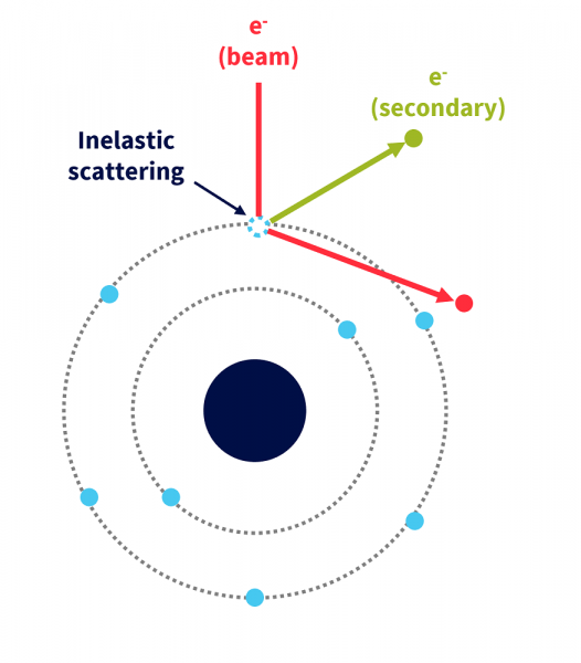
Secondary electrons are created through inelastic scattering of the electron beam with outer-shell electrons in the atoms of the surface. They typically have theses properties:

  • Low kinetic energy, <50 eV
  • Surface sensitive, only the top-most few nanometres
  • Small interaction area, good for high resolution
  • Best for topographic contrast

Back-scattered electrons are the initial electrons from the beam reflecting from the surface. They occur due to elastic scattering, where the electron trajectory is deflected due to interaction with the nucleus of the atom. Because it is elastic, they lose very little energy.

  • High kinetic energy, approximately the beam energy (e.g. 15 keV)
  • Sub-surface information from microns deep
  • Larger interaction area, poorer resolution
  • Gives material/compositional contrast

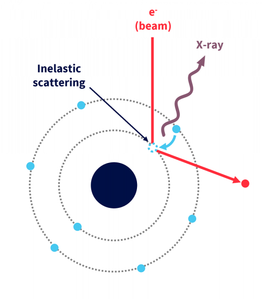
X-rays are created when the electron beam inelastically scatters from core-shell electrons. The atom will replace this scattered electron with one from a higher shell, and relax by releasing the excess energy as an X-ray photon. This X-ray has energy equal to the different in orbital energies, and therefore is characteristic of the atom.

  • Fingerprint for the elemental composition
  • Identifies elements and relative abundance
  • Largest interaction volume
  • Generally lower resolution signal

Information depth

Because of the different processes involved in generating these signals, they also have different interaction volumes, i.e. regions where the signals can come from.

  • Secondary electrons (SE) are very low energy, which means they cannot escape from deep within the sample, or away from where the beam is focussed. This means the SE signal will give you the best resolution, the best surface sensitivity, and is ideal for topographic contrast.

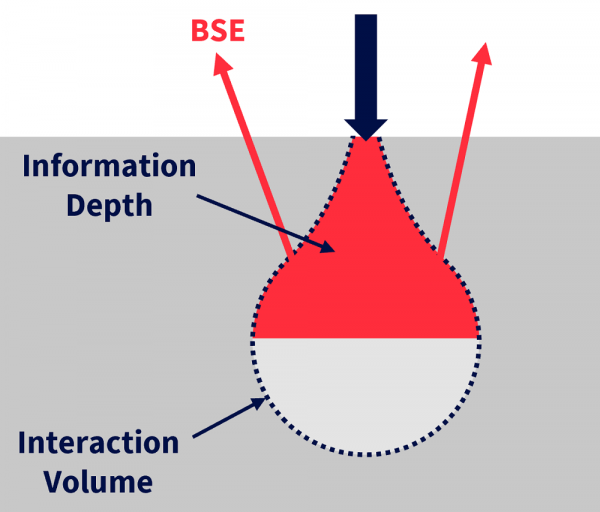
  • Back-scattered electrons (BSE) are high energy, and are effectively the electron beam bouncing elastically from the sample with no change in kinetic energy. This signal can carry information from microns deep into the sample, and can originate further away from the beam position. It gives you compositional contrast, but the resolution is not as good as the SE signal.

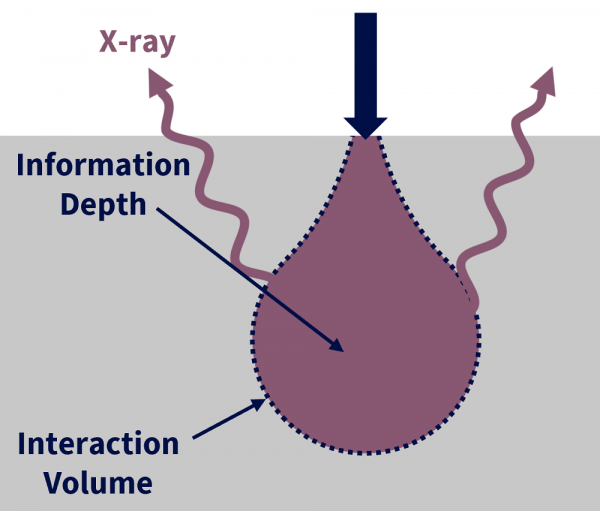
  • X-rays will easily travel through many microns of material, and thus this signal can originate from the deepest within the sample for a given electron beam energy. It gives the most rich information about elemental composition, but at much poorer resolution compared to both the SE and BSE signals.

Next - Vacuum modes

Back to MCFP Learning Home

Materials Characterisation and Fabrication Platform

  • Our Capabilities
    • Nanofabrication
    • Nanomaterials Characterisation
      • Atomic force microscopy
      • Anton Paar NHT3 Nanoindenter
      • DataPhysics optical contact angle
      • Hirox RH-2000 2D/3D microscope
      • Quorum Q150T Sputter Coater
    • Advanced Fluorescence Imaging
      • Zeiss Elyra 7 Lattice SIM
      • Nikon A1R+ Confocal Microscope (CLSM)
      • STORM (Stochastic optical reconstruction microscopy): Nikon N-STORM
      • Olympus IX71 Fluorescence Microscope
    • Cytometry and Particle Characterisation
      • Mass cytometry
      • Halo
      • NanoSight Pro
      • Apogee A-50 Microflow Cytometer
      • CytoFLEX Nano
      • Imaging Flow Cytometry
      • ICP-MS
      • Imaging ToF-ICP-MS
    • Electron and Ion Microscopy
      • Scanning electron microscopy (SEM)
      • Helium ion microscopy and dual-beam nanofabrication
      • Sample Preparation
    • X-Ray Characterisation
      • X-ray diffraction (XRD)
      • X-ray fluorescence (XRF)
    • Vibrational Spectroscopy
      • Confocal Raman Microspectroscopy
      • Fourier Transform Infrared Microscopy
    • Biological Optical Microscopy Platform (BOMP)
    • Ian Holmes Imaging Centre
    • Trace Analysis for Chemical, Earth and Environmental Sciences (TrACEES)
    • University of Melbourne Research Infrastructure
    • MCFP 2023 User Survey
  • Access Equipment
  • MCFP news and events
    • MCFP Image Competition
      • MCFP Image Competition
  • Our Expertise
    • Elena Taran
    • Anders Barlow
    • Paul Brannon
    • Darryl Johnson
    • Dan Smith
    • Raveen Wijesuriya
    • Tian Zheng
    • Ray Dagastine
    • George Franks
  • Services for Industry
  • MCFP Learning
    • Video Guides
      • LUMOS ATR-FTIR Guides
      • CytoFLEX Guides
      • NanoSight Guides
      • FlexSEM-EDS Guides
    • FlexSEM-EDS FAQs
  • Sustainability
    • Sustainability Framework
    • Sustainability on Campus
    • FEIT Sustainability
    • Green Impact
    • Sustainable ANFF
  • Publications
  • Current Students
  • Library
  • Staff

Acknowledgement of Country

We acknowledge Aboriginal and Torres Strait Islander people as the Traditional Owners of the unceded lands on which we work, learn and live. We pay respect to Elders past, present and future, and acknowledge the importance of Indigenous knowledge in the Academy.

Read about our Indigenous priorities

Site footer

  • About us
  • Careers at Melbourne
  • Safety and respect
  • Newsroom
  • Contact
  • Campus locations

Contact details

Phone 13 MELB (13 6352)
International +61 3 9035 5511

Address
The University of Melbourne
Grattan Street, Parkville
Victoria 3010
Australia

Connect with us

  • Emergency
  • Terms & privacy
  • Accessibility
  • Privacy
  • The University of Melbourne (Australian University): PRV12150
  • CRICOS number: 00116K
  • ABN: 84 002 705 224