  1. Materials Characterisation and Fabrication Platform
  2. MCFP Learning
  3. Scanning Electron Microscopy
  4. Getting good images
  5. Beam conditions
  • Scanning Electron Microscopy
  • Introduction
  • Applications of SEM
  • All Fundamentals of SEMThe sourceThe columnThe chamber and sample stageElectron interactions and detected signalsVacuum modes
  • All Getting good imagesSample preparationBeam conditionsChoosing the detectorFocussing and working distanceBrightness and contrastScan speedStigmatism
  • Get into the lab!

Beam conditions

Choice of beam conditions can have the most significant impact on the quality of images you can obtain in SEM. There are two parameters you will need to pay attention to:

  • Accelerating voltage, Vacc
  • Spot intensity

Accelerating Voltage

This parameter determines the kinetic energy of the electron beam used to probe your sample surface. For example, a 15 kV accelerating voltage results in an electron with 15 keV kinetic energy. Accelerating voltage, and thus beam energy, impacts the quality of your images in multiple ways.

Resolution Depth sensitivity Damage and charging

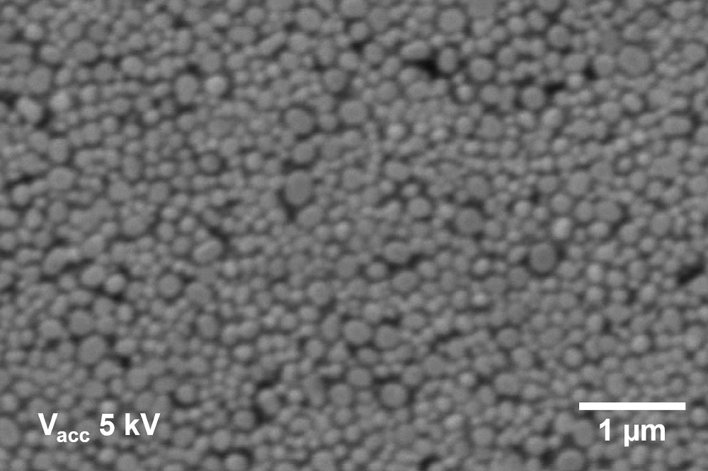
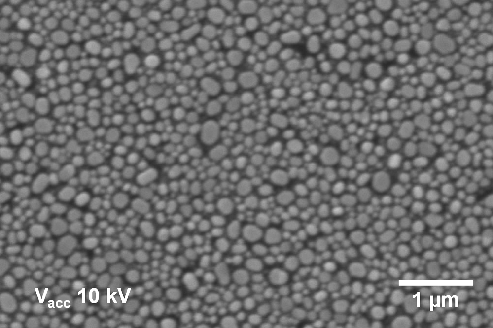
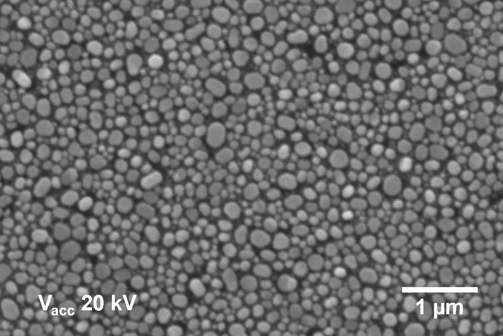
The kinetic energy of the beam determines its ability to distinguish between small objects, i.e. resolution. Generally:

  • Higher Vacc gives better resolution
  • Lower Vacc gives poorer resolution

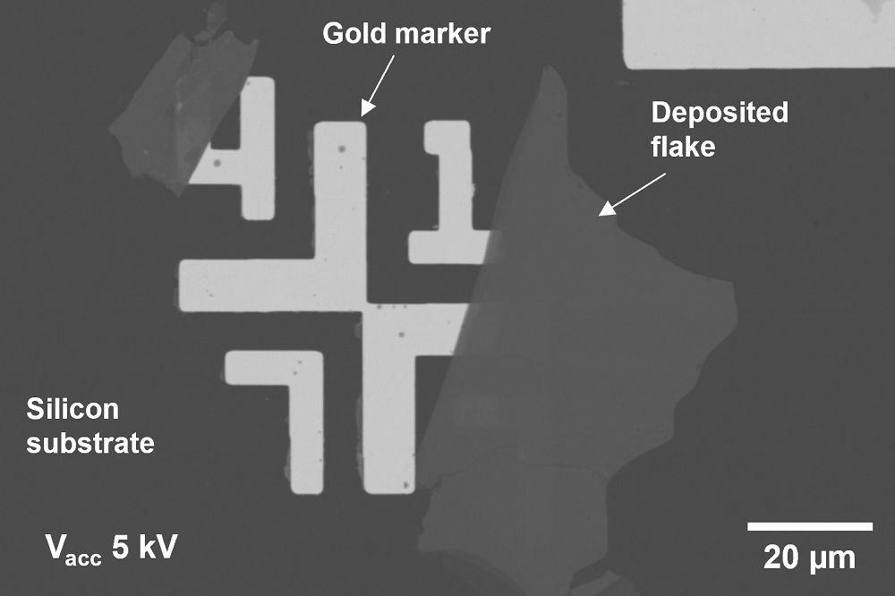
How deep into a sample surface the electron beam travels is also impacted by its energy:

  • Higher Vacc results in deeper information
  • Lower Vacc results in more surface information

Higher energies can lead to damage of soft materials, and also make charging issues worse on poor conductors:

  • Higher Vacc increases damage and charging
  • Lower Vacc reduces damage and charging

These images show how changing the accelerating voltage impacts the resolution of the SEM. Increasing the voltage improves the sharpness of the images.

  • SEM at 5kV
  • SEM at 10kV
  • SEM at 20kV

These images demonstrate the change in depth sensitivity with accelerating voltage. At high beam energy the technique "see through" thin materials on a surface. Reducing the accelerating voltage improves the contrast for thin flakes and 2D nanomaterials.
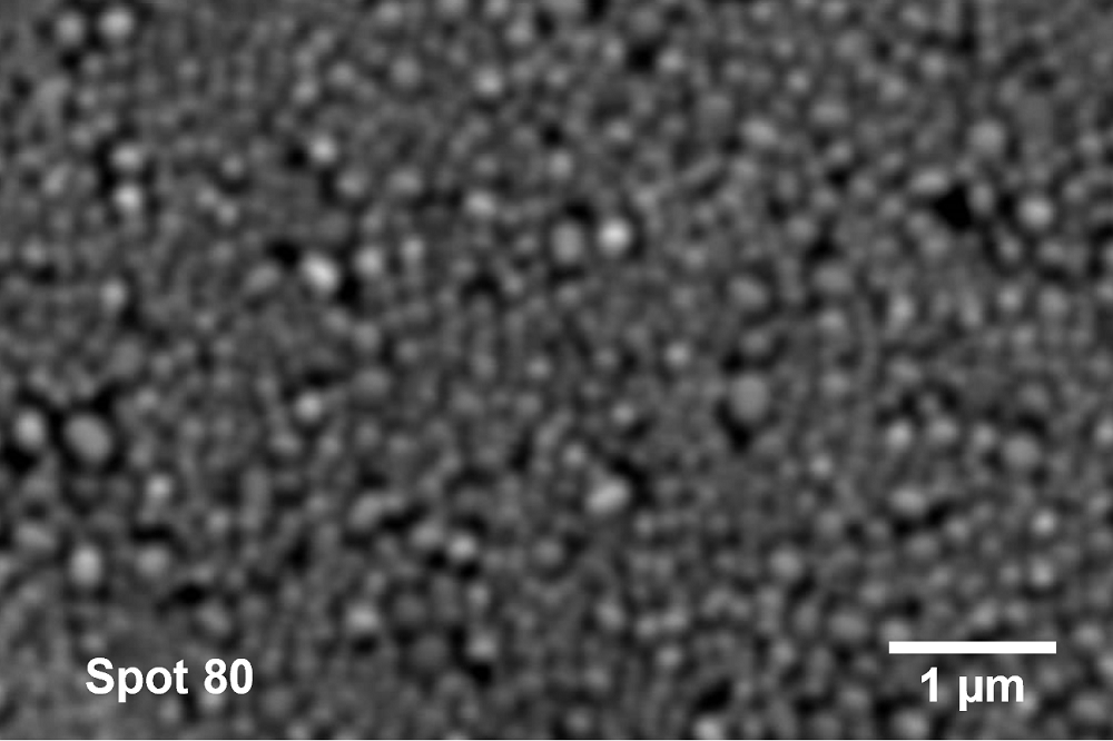
  • SEM depth sensitivity at 15kV
    Imaging at 15kV results in deeper information, losing contrast of thin deposited materials on a surface
  • SEM depth information at 5kV
    Imaging at 5kV improves the surface sensitivity of the technique, giving better contrast to deposited 2D nanomaterial flakes

Spot Intensity

The condenser lens controls how much of the electron beam passes through the column, and this is controlled b ythe spot intensity. In simple terms, this parameter controls the size and brightness of the electron spot on the sample when in focus. Your choice of spot intensity will depend on the sample, the feature sizes you are interested in imaging, and the signal you wish to measure.

Low spot intensity (10-40) High spot intensity (60-80)
  • Smaller spot size giving sharper image resolution
  • Lower current results in less signal generated
  • Reduces damage and charging
  • Larger spot size giving poorer image resolution
  • High current results in more signal generated
  • Can increase damage and charging
  • SEM at Spot 20
  • SEM at Spot 50
  • SEM at Spot 80

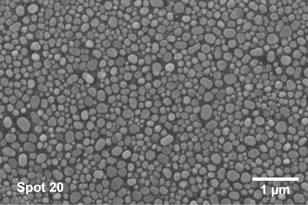
Quick Guide to Beam Conditions

  • Here we want to maximise resolution:

    • Choose a high Vacc, e.g. 15-20 kV
    • Choose a lower Spot Intensity, e.g. 20-40
  • In VP-SEM mode we usually need to compensate for signal so we usually use a higher Spot Intensity:

    • Choose a high Vacc, e.g. 15-20 kV
    • Choose a mid-range Spot Intensity, e.g. 40-60
  • To increase surface sensitivity we reduce Vacc and compensate with an increase in Spot Intensity:

    • Choose a lower Vacc, e.g. 5-10 kV
    • Choose a mid-range Spot Intensity, e.g. 40-60
  • To optimise for EDS we want to start with 15 keV (3× most X-ray energies) and boost our signal with high Spot Intensity:

    • Choose a Vacc of 15 kV to start
    • Choose a higher Spot Intensity, e.g. 60-80
    • You can adjust the Vacc to control surface sensitivity

Next - Choosing the right detector

Back to MCFP Learning Home

Materials Characterisation and Fabrication Platform

  • Our Capabilities
    • Nanofabrication
    • Nanomaterials Characterisation
      • Atomic force microscopy
      • Anton Paar NHT3 Nanoindenter
      • DataPhysics optical contact angle
      • Hirox RH-2000 2D/3D microscope
      • Quorum Q150T Sputter Coater
    • Advanced Fluorescence Imaging
      • Zeiss Elyra 7 Lattice SIM
      • Nikon A1R+ Confocal Microscope (CLSM)
      • STORM (Stochastic optical reconstruction microscopy): Nikon N-STORM
      • Olympus IX71 Fluorescence Microscope
    • Cytometry and Particle Characterisation
      • Mass cytometry
      • Halo
      • NanoSight Pro
      • Apogee A-50 Microflow Cytometer
      • CytoFLEX Nano
      • Imaging Flow Cytometry
      • ICP-MS
      • Imaging ToF-ICP-MS
    • Electron and Ion Microscopy
      • Scanning electron microscopy (SEM)
      • Helium ion microscopy and dual-beam nanofabrication
      • Sample Preparation
    • X-Ray Characterisation
      • X-ray diffraction (XRD)
      • X-ray fluorescence (XRF)
    • Vibrational Spectroscopy
      • Confocal Raman Microspectroscopy
      • Fourier Transform Infrared Microscopy
    • Biological Optical Microscopy Platform (BOMP)
    • Ian Holmes Imaging Centre
    • Trace Analysis for Chemical, Earth and Environmental Sciences (TrACEES)
    • University of Melbourne Research Infrastructure
    • MCFP 2023 User Survey
  • Access Equipment
  • MCFP news and events
    • MCFP Image Competition
      • MCFP Image Competition
  • Our Expertise
    • Elena Taran
    • Anders Barlow
    • Paul Brannon
    • Darryl Johnson
    • Dan Smith
    • Raveen Wijesuriya
    • Tian Zheng
    • Ray Dagastine
    • George Franks
  • Services for Industry
  • MCFP Learning
    • Video Guides
      • LUMOS ATR-FTIR Guides
      • CytoFLEX Guides
      • NanoSight Guides
      • FlexSEM-EDS Guides
    • FlexSEM-EDS FAQs
  • Sustainability
    • Sustainability Framework
    • Sustainability on Campus
    • FEIT Sustainability
    • Green Impact
    • Sustainable ANFF
  • Publications
  • Current Students
  • Library
  • Staff

Acknowledgement of Country

We acknowledge Aboriginal and Torres Strait Islander people as the Traditional Owners of the unceded lands on which we work, learn and live. We pay respect to Elders past, present and future, and acknowledge the importance of Indigenous knowledge in the Academy.

Read about our Indigenous priorities

Site footer

  • About us
  • Careers at Melbourne
  • Safety and respect
  • Newsroom
  • Contact
  • Campus locations

Contact details

Phone 13 MELB (13 6352)
International +61 3 9035 5511

Address
The University of Melbourne
Grattan Street, Parkville
Victoria 3010
Australia

Connect with us

  • Emergency
  • Terms & privacy
  • Accessibility
  • Privacy
  • The University of Melbourne (Australian University): PRV12150
  • CRICOS number: 00116K
  • ABN: 84 002 705 224