  1. Materials Characterisation and Fabrication Platform
  2. MCFP Learning
  3. Scanning Electron Microscopy
  4. Fundamentals of SEM
  5. The source
  • Scanning Electron Microscopy
  • Introduction
  • Applications of SEM
  • All Fundamentals of SEMThe sourceThe columnThe chamber and sample stageElectron interactions and detected signalsVacuum modes
  • All Getting good imagesSample preparationBeam conditionsChoosing the detectorFocussing and working distanceBrightness and contrastScan speedStigmatism
  • Get into the lab!

The source

At the top of our SEM is the electron source. This is where the beam of electrons is first generated before being directed down the electron column towards the sample. Many SEM instruments you encounter will be designated by the type of source that they have. This is because the source determines both the ultimate performance of an SEM, and also the requirements of that SEM. No matter the type of source though, the electron beam is generated in largely the same way.

There are two groups of electron sources in SEM: thermionic emitters, and field emitters. Thermionic emitters rely on heating a source up to a high temperature, which promotes the spontaneous emission of electrons from the source material. These will commonly be tungsten hairpin filament sources, or hexaboride crystal emitters. Field emitters use a very intense electric field to pull the electrons directly from the source material.

Types of electron sources

Tungsten filament Hexaboride crystal Field-emission (FE)

The tungsten filament is a thermionic emitter. That is, electron emission is stimulated by heating the filament with electric current. It is the simplest of the electron sources. It is affordable, robust, easy to exchange and align, and amenable to working in variable pressure environments.

However it has the lowest brightness of all the sources, does not achieve as high an ultimate resolution, and has a relatively short lifetime.

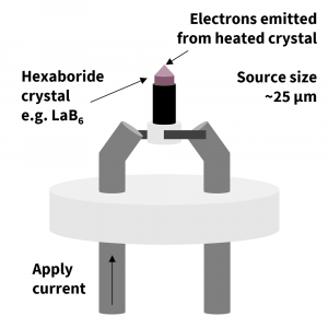
Hexaboride crystals, such as LaB6 and CeB6, are also thermionic emitters, like tungsten. But these sources are brighter, meaning the electron beam current is greater than tungsten, and they can achieve better resolution as the region where the electrons are emitted from is smaller.

But increased performance comes with increased requirements, and these sources need better vacuum conditions maintained around the source region. It means they also have longer lifetimes, but at higher cost, so tend to be found on the more expensive instruments.

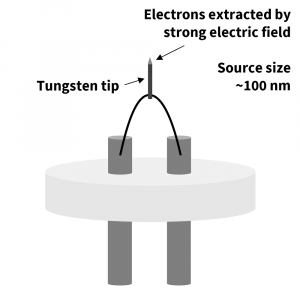
The field-emission source is the highest performance source for an SEM. Instruments that utilise these are often specifically marketed as FE-SEM to designate this performance. They are the brightest source, maintain longest lifetime, and give the best resolution.

But they require the greatest vacuum conditions, often high-vacuum in the source at all times, and are generally found only on high-end SEM instruments.

Our electron source sits inside a cylinder called a Wehnelt cap, and this sits above the anode. The Wehnelt is held at a negative voltage, while the anode is held at a positive voltage. These two components work together to direct the electron beam emitted from the source down into the optics of the electron column. It is the strength of the voltage applied to the anode that determines your electron beam energy.

On the FlexSEM this is presented as Vacc, or accelerating voltage, and the energy of your beam will be in electron-volts, or eV. For example, a 15 kV accelerating voltage gives you a 15 keV energy electron beam. This becomes important later when we discuss electron-surface interactions.

Next - The column

Back to MCFP Learning Home

Materials Characterisation and Fabrication Platform

  • Our Capabilities
    • Nanofabrication
    • Nanomaterials Characterisation
      • Atomic force microscopy
      • Anton Paar NHT3 Nanoindenter
      • DataPhysics optical contact angle
      • Hirox RH-2000 2D/3D microscope
      • Quorum Q150T Sputter Coater
    • Advanced Fluorescence Imaging
      • Zeiss Elyra 7 Lattice SIM
      • Nikon A1R+ Confocal Microscope (CLSM)
      • STORM (Stochastic optical reconstruction microscopy): Nikon N-STORM
      • Olympus IX71 Fluorescence Microscope
    • Cytometry and Particle Characterisation
      • Mass cytometry
      • Halo
      • NanoSight Pro
      • Apogee A-50 Microflow Cytometer
      • CytoFLEX Nano
      • Imaging Flow Cytometry
      • ICP-MS
      • Imaging ToF-ICP-MS
    • Electron and Ion Microscopy
      • Scanning electron microscopy (SEM)
      • Helium ion microscopy and dual-beam nanofabrication
      • Sample Preparation
    • X-Ray Characterisation
      • X-ray diffraction (XRD)
      • X-ray fluorescence (XRF)
    • Vibrational Spectroscopy
      • Confocal Raman Microspectroscopy
      • Fourier Transform Infrared Microscopy
    • Biological Optical Microscopy Platform (BOMP)
    • Ian Holmes Imaging Centre
    • Trace Analysis for Chemical, Earth and Environmental Sciences (TrACEES)
    • University of Melbourne Research Infrastructure
    • MCFP 2023 User Survey
  • Access Equipment
  • MCFP news and events
    • MCFP Image Competition
      • MCFP Image Competition
  • Our Expertise
    • Elena Taran
    • Anders Barlow
    • Paul Brannon
    • Darryl Johnson
    • Dan Smith
    • Raveen Wijesuriya
    • Tian Zheng
    • Ray Dagastine
    • George Franks
  • Services for Industry
  • MCFP Learning
    • Video Guides
      • LUMOS ATR-FTIR Guides
      • CytoFLEX Guides
      • NanoSight Guides
      • FlexSEM-EDS Guides
    • FlexSEM-EDS FAQs
  • Sustainability
    • Sustainability Framework
    • Sustainability on Campus
    • FEIT Sustainability
    • Green Impact
    • Sustainable ANFF
  • Publications
  • Current Students
  • Library
  • Staff

Acknowledgement of Country

We acknowledge Aboriginal and Torres Strait Islander people as the Traditional Owners of the unceded lands on which we work, learn and live. We pay respect to Elders past, present and future, and acknowledge the importance of Indigenous knowledge in the Academy.

Read about our Indigenous priorities

Site footer

  • About us
  • Careers at Melbourne
  • Safety and respect
  • Newsroom
  • Contact
  • Campus locations

Contact details

Phone 13 MELB (13 6352)
International +61 3 9035 5511

Address
The University of Melbourne
Grattan Street, Parkville
Victoria 3010
Australia

Connect with us

  • Emergency
  • Terms & privacy
  • Accessibility
  • Privacy
  • The University of Melbourne (Australian University): PRV12150
  • CRICOS number: 00116K
  • ABN: 84 002 705 224