  1. Materials Characterisation and Fabrication Platform
  2. MCFP Learning
  3. Scanning Electron Microscopy
  4. Introduction
  • Scanning Electron Microscopy
  • Introduction
  • Applications of SEM
  • All Fundamentals of SEMThe sourceThe columnThe chamber and sample stageElectron interactions and detected signalsVacuum modes
  • All Getting good imagesSample preparationBeam conditionsChoosing the detectorFocussing and working distanceBrightness and contrastScan speedStigmatism
  • Get into the lab!

Introduction

What is a Scanning Electron Microscope?

A scanning electron microscope, or SEM, uses a focused beam of electrons to investigate a sample under analysis, and create a high magnification image of its surface. This image is created in a different way to a bench top optical microscope that you might already be familiar with. The "scanning" part of SEM refers to the electron beam being scanned left-to-right, top-to-bottom, across the sample. At each position where the beam is located, the SEM reads the signal coming back from the sample, before moving to the next position. Pixel by pixel and line by line, the SEM puts these signals together to create an image, enabling us to see the surface.

SEM allows us to view the world at much smaller scales (higher magnification) than we can with our eyes or even with a light microscope. With an SEM we can magnify surfaces as much as 10,000× or more, to see fine details such as the size of pores in a drug-delivery nanoparticles, the thickness of coatings on food packaging, or the ultra-fine hairs in the inner ear that allow you to hear sounds.

An SEM can range in size, from benchtop instruments not much bigger than a desktop PC, mid-sized instruments that balance performance with ease of use and functionality, to full-sized instrument that benefit from dedicated rooms and experienced operators.

No matter the size of the instrument they all fundamentally operate in the same way. All SEM instruments require vacuum conditions, they will all have an electron source that generates the beam, and an electron column that focuses and rasters the beam, and they all have a way of mounting your sample and moving it around remotely inside the vacuum chamber (the sample stage). The key difference is in their ease of use, their performance (such as imaging resolution) their capability (i.e. what signals can be detected), and of course, the cost!

This is your SEM

The MCFP operates a Hitachi FlexSEM SU1000 variable pressure scanning electron microscope. The FlexSEM is a powerful and versatile SEM, in a fast and user-friendly package. You can explore its features below.

  • The MCFP FlexSEM
    The MCFP's Hitachi FlexSEM Scanning Electron Microscope
  • FlexSEM 45 degree tilt
    The FlexSEM stage can tilt to enable cross-section imaging
  • FlexSEM multiple samples
    Multiple samples can be mounted in the FlexSEM
  • Embedded samples mounted
    The FlexSEM can secure embedded and unusually shaped samples
Operating Modes Detectable signals Sample handling Stage motion Performance

The FlexSEM can operate in two vacuum modes, depending on the needs of your sample and analysis:

  • High Vacuum mode - for the best performance
  • Variable Pressure mode - for maximum flexibility

The FlexSEM is configured with multiple detectors:

  • Secondary Electrons - for resolution
  • Back-Scattered Electrons - for material contrast
  • Ultra-Variable Detector - for resolution in VP mode
  • X-rays - for elemental identification
  • Cathodoluminescence - for crystal structures

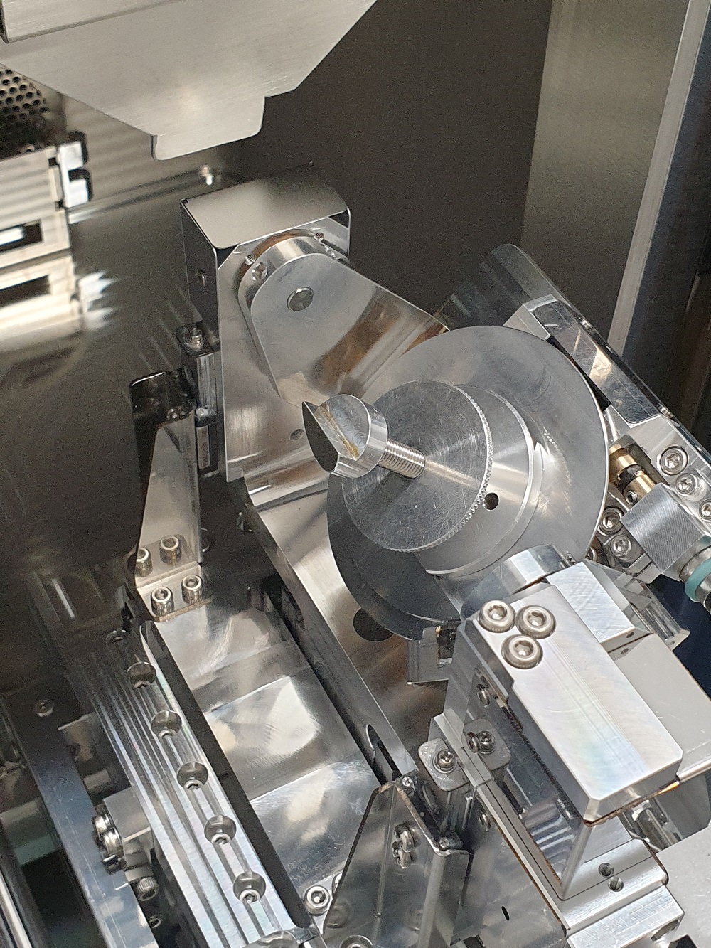
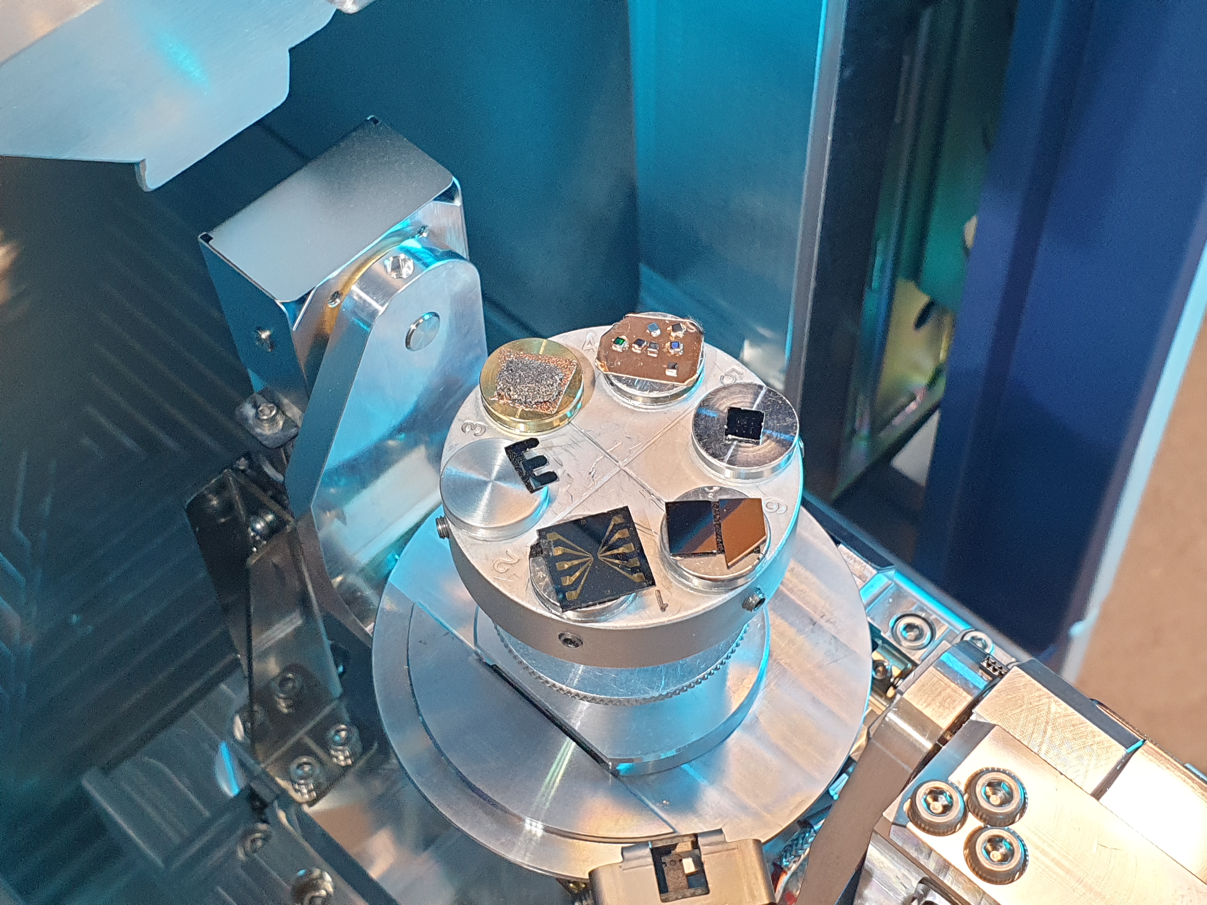
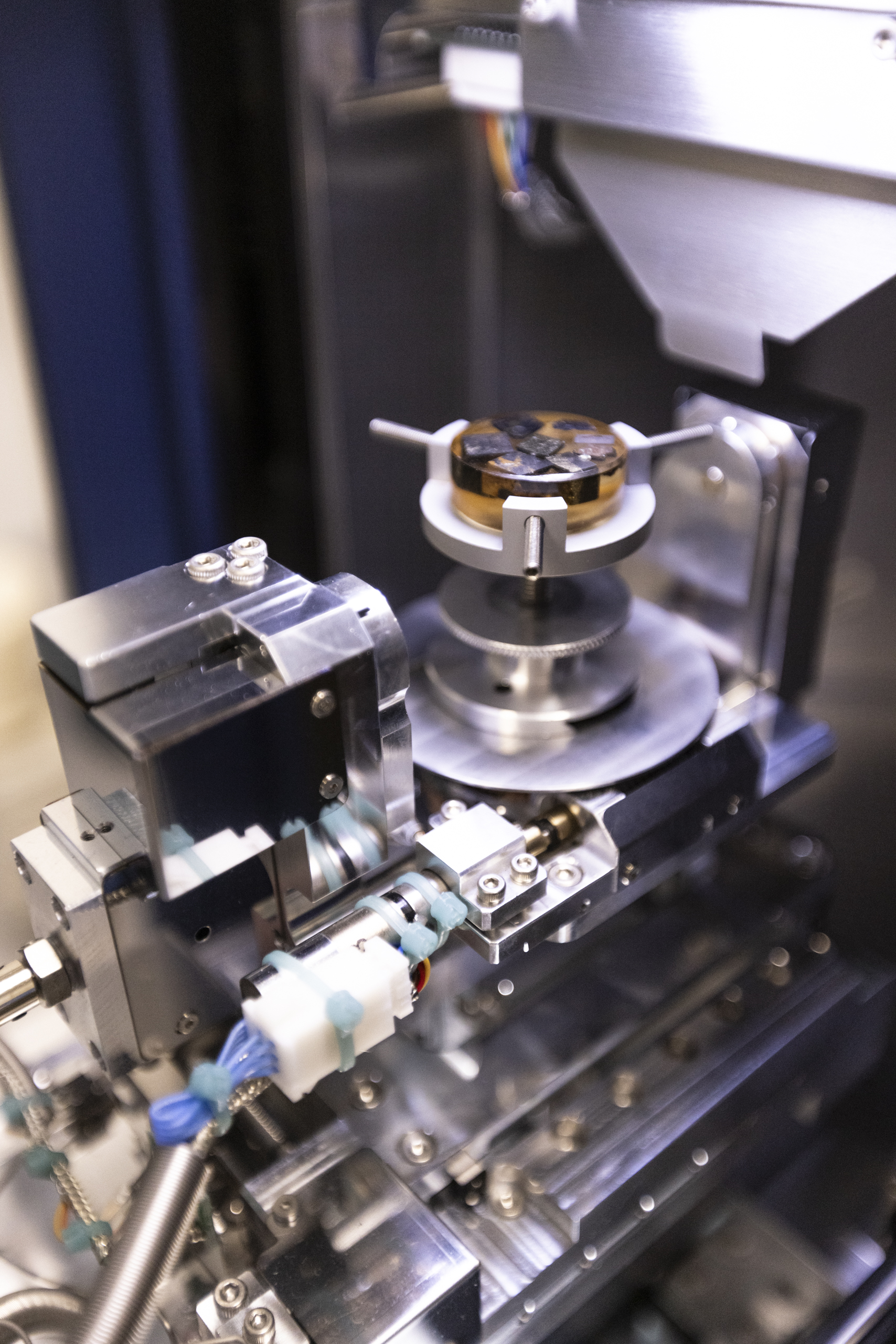
The FlexSEM can mount almost any sample you could think of:

  • Large flat samples
  • Tall skinny samples
  • Powders, fibres, loose material
  • Multiple pin stubs
  • Irregular samples

The FlexSEM stage can move in 5 directions

  • X and Y is your lateral motion, to move around on samples
  • Z is your height, this changes working distance
  • Tilt (T) and Rotation (R) allow you to change your viewing perspective

The FlexSEM is a powerful SEM in a small and easy package:

  • Tungsten thermionic source
  • 4 nm ultimate resolution
  • Up to ×300,000 magnification

Don't worry if you don't know what all of those terms mean just yet, throughout this module you will learn all about the fundamentals of SEM, and we will cover everything related to the FlexSEM and its capability.

Next - Applications of SEM

Back to MCFP Learning Home

Materials Characterisation and Fabrication Platform

  • Our Capabilities
    • Nanofabrication
    • Nanomaterials Characterisation
      • Atomic force microscopy
      • Anton Paar NHT3 Nanoindenter
      • DataPhysics optical contact angle
      • Hirox RH-2000 2D/3D microscope
      • Quorum Q150T Sputter Coater
    • Advanced Fluorescence Imaging
      • Zeiss Elyra 7 Lattice SIM
      • Nikon A1R+ Confocal Microscope (CLSM)
      • STORM (Stochastic optical reconstruction microscopy): Nikon N-STORM
      • Olympus IX71 Fluorescence Microscope
    • Cytometry and Particle Characterisation
      • Mass cytometry
      • Halo
      • NanoSight Pro
      • Apogee A-50 Microflow Cytometer
      • CytoFLEX Nano
      • Imaging Flow Cytometry
      • ICP-MS
      • Imaging ToF-ICP-MS
    • Electron and Ion Microscopy
      • Scanning electron microscopy (SEM)
      • Helium ion microscopy and dual-beam nanofabrication
      • Sample Preparation
    • X-Ray Characterisation
      • X-ray diffraction (XRD)
      • X-ray fluorescence (XRF)
    • Vibrational Spectroscopy
      • Confocal Raman Microspectroscopy
      • Fourier Transform Infrared Microscopy
    • Biological Optical Microscopy Platform (BOMP)
    • Ian Holmes Imaging Centre
    • Trace Analysis for Chemical, Earth and Environmental Sciences (TrACEES)
    • University of Melbourne Research Infrastructure
    • MCFP 2023 User Survey
  • Access Equipment
  • MCFP news and events
    • MCFP Image Competition
      • MCFP Image Competition
  • Our Expertise
    • Elena Taran
    • Anders Barlow
    • Paul Brannon
    • Darryl Johnson
    • Dan Smith
    • Raveen Wijesuriya
    • Tian Zheng
    • Ray Dagastine
    • George Franks
  • Services for Industry
  • MCFP Learning
    • Video Guides
      • LUMOS ATR-FTIR Guides
      • CytoFLEX Guides
      • NanoSight Guides
      • FlexSEM-EDS Guides
    • FlexSEM-EDS FAQs
  • Sustainability
    • Sustainability Framework
    • Sustainability on Campus
    • FEIT Sustainability
    • Green Impact
    • Sustainable ANFF
  • Publications
  • Current Students
  • Library
  • Staff

Acknowledgement of Country

We acknowledge Aboriginal and Torres Strait Islander people as the Traditional Owners of the unceded lands on which we work, learn and live. We pay respect to Elders past, present and future, and acknowledge the importance of Indigenous knowledge in the Academy.

Read about our Indigenous priorities

Site footer

  • About us
  • Careers at Melbourne
  • Safety and respect
  • Newsroom
  • Contact
  • Campus locations

Contact details

Phone 13 MELB (13 6352)
International +61 3 9035 5511

Address
The University of Melbourne
Grattan Street, Parkville
Victoria 3010
Australia

Connect with us

  • Emergency
  • Terms & privacy
  • Accessibility
  • Privacy
  • The University of Melbourne (Australian University): PRV12150
  • CRICOS number: 00116K
  • ABN: 84 002 705 224