Sample preparation
Careful consideration for how you present your sample to the SEM will maximise your chances of getting good images and results from your session. Keep the following considerations in mind when preparing your sample:
- The conductivity of your sample/substrate
- The moisture content of your sample
- Secure mounting of your sample to the holder
- Thoughtful positioning of your region of interest to the beam and the detectors on the instrument
Sample Conductivity
Ideally a sample presented to an SEM should be conductive. This is because an SEM uses a beam of electrons that impart charge into your sample surface. Conductive samples, like metals, can easily dissipate this charge through the material, causing no issues. Poorly or non-conducting samples, like polymers, ceramics, and glass, do not allow this easy flow of electrons within the material. This leads to a build up of negative charge where the beam is scanned. Because the signals we detect are also electrons, they are impacted by this surface charge and the result is artefacts and distortions in the image.
A common approach to enable imaging of non-conductive samples is not apply a very thin, typically 5-30nm, coating of metal such as gold or platinum on the sample surface to create a conductive surface, allowing the charge to dissipate. This has the added bonus of enhancing edge contrast when using the secondary electron detector, but can mask some material contrast when using the back-scattered electron detector. The coating will also be detectable in X-ray analysis.
An alternative approach with the FlexSEM is to operate in the variable pressure (VP) vacuum mode, allowing many poorly conducting samples to be imaged, but just remember that this limits your choice of detectors, and can have an impact on signal and resolution.
Moisture Content
An ideal SEM sample will be free from oils and moisture. This is because we want to operate in a high-vacuum environment where moisture and oils could become volatile and create artefacts or even cause damage to the instrument.
Biological specimens, or samples that have been stored in liquid such as water/ethanol, generally need to be dried before mounting for SEM analysis. For some samples a simple approach is air-drying in ambient conditions or with a stream of dry nitrogen, however for many biological samples this is not suitable as the drying process deforms the microscopic structure of the sample.
Chemical fixation followed by freeze drying or critical point drying is usually the preferred approach to dehydrate most biological samples for imaging. These samples should also be coated soon after drying, and imaged as soon as possible after preparation.
Sample Mounting
All samples need to be securely held in place to eliminate motion during imaging. Most of the time we would mount a sample onto an SEM "pin stub", but samples can also be mounted directly to sample holders. Mounting is usually achieved using conductive double-sided tape, conductive paste, or metal clips.
Solids such as metals, pieces of silicon wafer, glass slides, or polymer films/membranes, can usually be mounted directly to a pin stub or holder using tape or clips. Tape is simple and convenient, clips can be tricky but offer a good mechanical hold and conductive path. Use a small amount of tape, and press the sample carefully onto the holder being sure not to damage your area of interest.
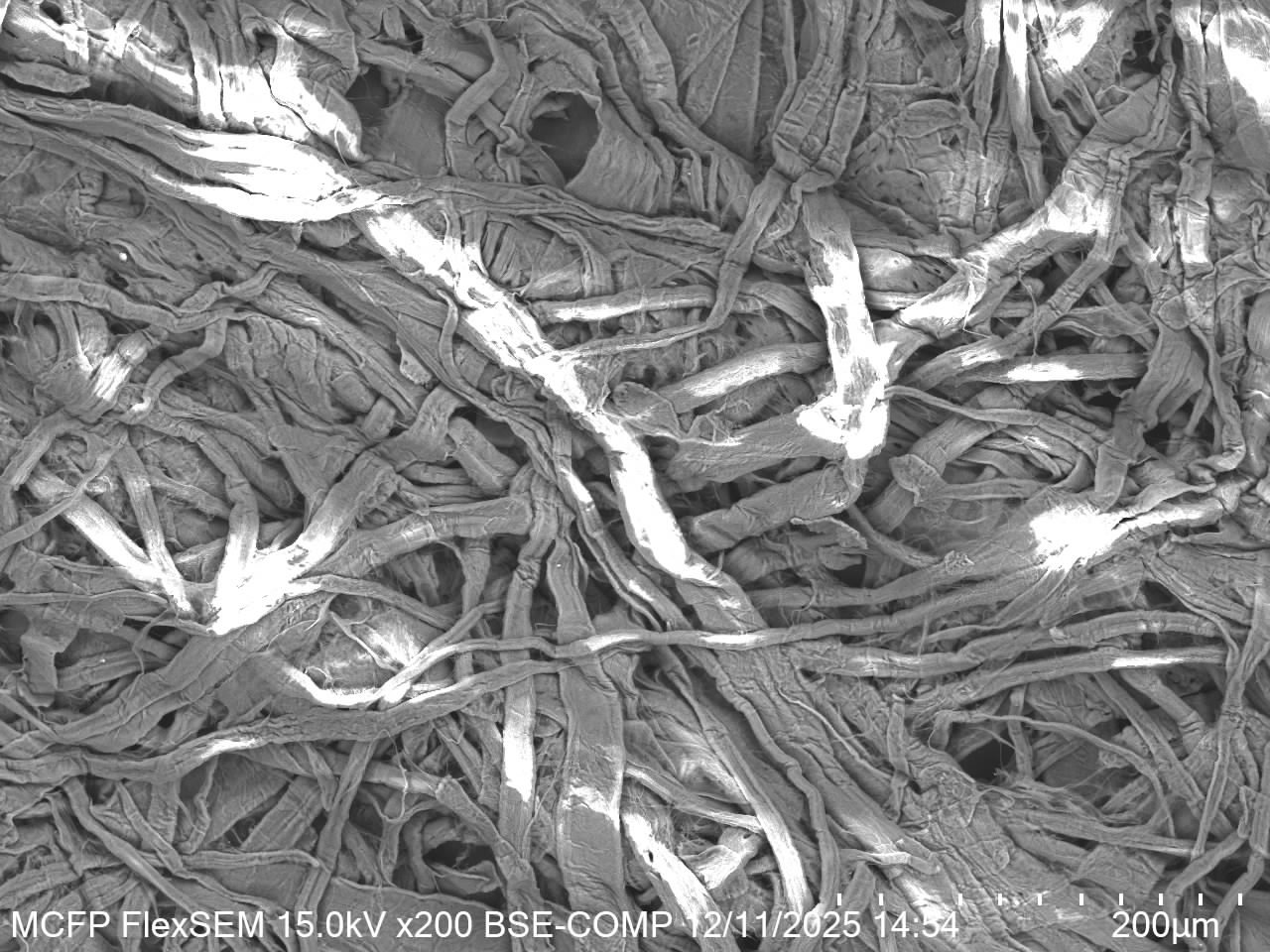
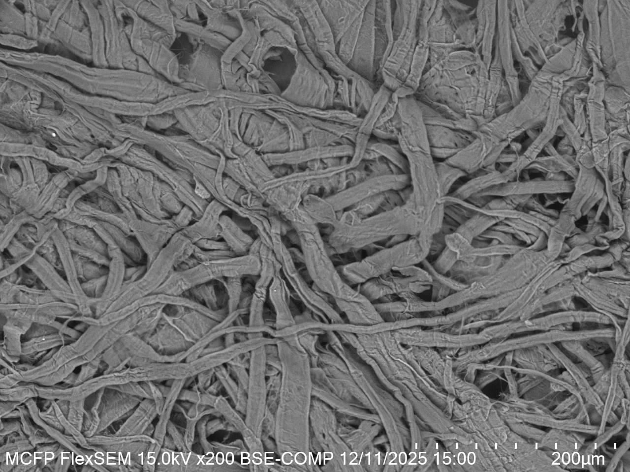
Powders, particulates, and fibres should be mounted onto a pin stub using adhesive tape. Apply a small amount of sample onto the tape on the stub, and then tap the stub on its side onto tissue to remove loose material. It is best not to mount multiple samples of this type onto a single holder to minimise cross-contamination.
Particulates in solution can also be drop-cast onto another substrate, such as silicon, to create an adhered film for imaging. Ensure the films is well-dried, and then mount the substrate as though it was a solid sample.
When mounting your samples consider the orientation of your region of interest relative to the beam and the detectors. There are multiple holders that allow you to mount at an angle to see edges and cross-sections for example.
Quick Guide for Sample Preparation
-
- Ensure sample is free from moisture and oils
- No coating should be necessary
- Mount the sample to a sample holder or pin stub using adhesive tape or clips
-
For loose dry particulates:
- Apply a small amount of the particulate sample to carbon tape
- Tap the pin stub on its side on tissue to dislodge loose particulates
- If desired, coat the sample, or use VP-SEM mode
For particulates in solution:
- Drop cast the solution onto a substrate such as a piece of silicon wafer and allow it to dry
- If desired, coat the sample, or use VP-SEM mode
-
- Mount the sample using adhesive tape
- If no coating is preferred, use the VP-SEM mode
- For high magnification and best results coat the sample and use the high-vacuum SEM mode
-
- Fix and dehydrate the sample
- Mount the specimen using carbon tape
- If no coating is preferred, use the VP-SEM mode
- For high magnification and best results coat the sample and use the high-vacuum SEM mode
-
- Use a 45° or 90° pre-tilted stub to mount your sample on its side, ideally using clips, but tape will suffice
- Ensure you have positioned your region of interest so that it will be visible in the SEM