Stigmatism
When an electron beam is focussed tightly to a spot, ideally that spot would have a circular shape. As the spot is rastered across the features on our sample, that circular shape is imparted into the images. As the beam goes in and out of focus (over or under focus), the circular spot would simply get larger and smaller, leading to uniformly soft or blurry images.
However no SEM optical system is perfect, and instead what tends to happen is that a beam can have an elliptical shape, rather than circular. This elliptical beam shape is instead imparted into images when out of focus, leading to a strange-looking distortion of the image features, and it limits the ultimate sharpness that can be achieved since the beam spot cannot be focussed to it smallest size.
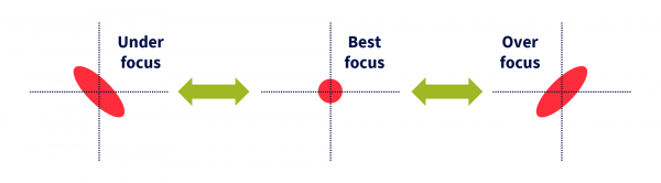
This is called astigmatism. Correcting beam stigmatism takes some practise, and can be one of the more challenging artefacts to identify and resolve, but it becomes important at high magnification to get the best possible images.
-
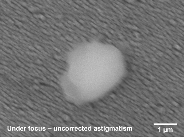
Astigmatism in SEM appears as streaking or smearing of image features in a specific direction orthogonal in under and over focus, here top-left to bottom-right -

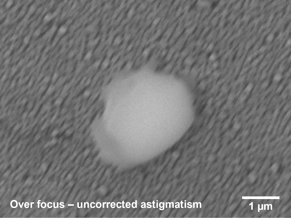
Astigmatism in SEM appears as streaking or smearing of image features in a specific direction orthogonal in under and over focus, here bottom-left to top-right -
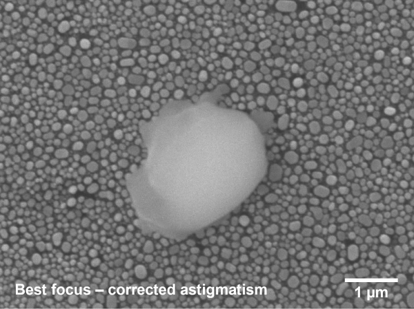
When astigmatism is corrected the best focus can be achieved, and uniform circular blurriness is observed in under and over-focussed images.


Guide to Correcting Astigmatism
- Determine if it is necessary to correct for astigmatism
- If you are capturing images at magnifications of less than ×5000 you may not see significant impact from astigmatism, in which case just ensure stigmators are reset or near zero adjustment
- If you are capturing images at magnifications greater than ×5000, you should check the stigmator settings
- Stigmators should be set at high magnification, with high contrast features that have rounded edges or at least edges in both vertical and horizontal directions in the image
- Use the Reduce Scan window, and ideally use the SE detector in high vacuum mode
- BSE detector in VP-SEM mode can be used, it just may be more challenging to optimise
- Reset stigmators to zero (centre) position
- Find best focus with Fine Focus
- Find best focus with X Stigmator
- Find best focus with Y Stigmator
- Iterate Steps 5 - 7 around a few times to optimise the focus