  1. Materials Characterisation and Fabrication Platform
  2. MCFP Learning
  3. Scanning Electron Microscopy
  4. Fundamentals of SEM
  5. The chamber and sample stage
  • Scanning Electron Microscopy
  • Introduction
  • Applications of SEM
  • All Fundamentals of SEMThe sourceThe columnThe chamber and sample stageElectron interactions and detected signalsVacuum modes
  • All Getting good imagesSample preparationBeam conditionsChoosing the detectorFocussing and working distanceBrightness and contrastScan speedStigmatism
  • Get into the lab!

The chamber and sample stage

The electron column is positioned directly above the stage. This is where you will mount your samples for analysis, and the stage enables you to move the sample around in multiple directions. The entire system is then enclosed by the vacuum chamber. This seals everything in and allows the vacuum pumps to reduce the pressure inside the SEM.

The need for vacuum

An SEM cannot operate at atmospheric pressure. The electron source will burn out almost immediately, and even if it could operate for long enough, the electrons that are emitted simply would not make it down to the sample without colliding with gas molecules in the atmosphere. So an SEM must operate under a low pressure, called vacuum, so that the source can maintain stable operation over a long period of time, and both the electron beam and the electron signal from the sample can travel through the chamber unimpeded.

Some systems can operate in intermediate modes, called variable pressure (VP-SEM) or environmental (E-SEM) SEMs, but they still require some level of vacuum to be maintained.

Vacuum is most commonly achieved by a combination of a backing pump and a turbo pump. This will usually be the noise you hear when the SEM is powered on.

The sample stage

Your samples will be mounted to a special holder that attaches to the stage inside the SEM. The stage will allow you to navigate around on your sample surface and change between samples. The stage also ensures that you have a good electrical connection to the instrument ground, allowing accumulated charge from the electron beam to flow out of the sample and minimise surface charging. An SEM stage will commonly have 5 axes of motion:
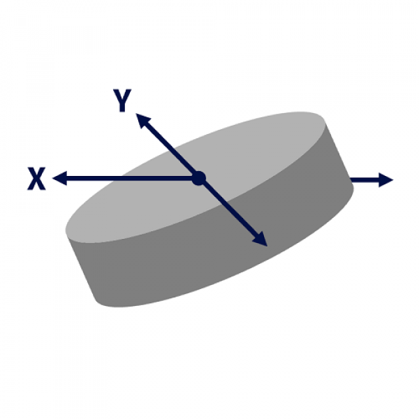
X and Y - lateral motion Z - height T - tilt R - rotate

This allows you to navigate around on your sample, or between samples, to find your regions of interest.
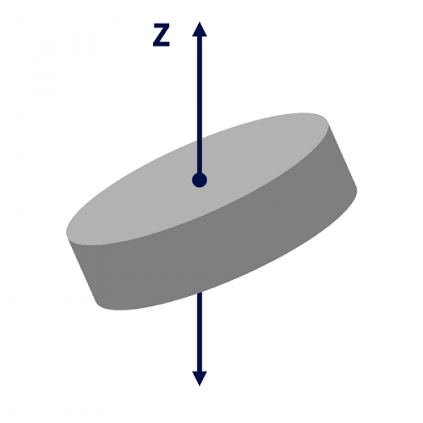
This allows you to vary the working distance, to increase your field of view, or to optimise for a different detector, like an EDS detector.
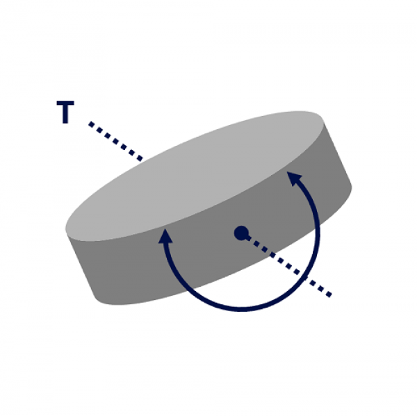
This allows you to tilt the sample relative to the viewing angle, giving a different perspective. It will usually be used to look at the sides or edges of samples.
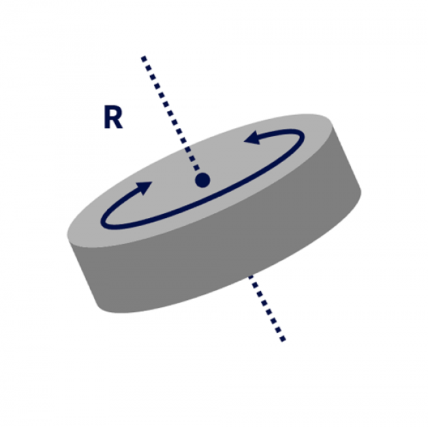
Not so commonly needed, but the rotation axis can help to align features to the field of view, or to better position a region in the view of a specific detector.
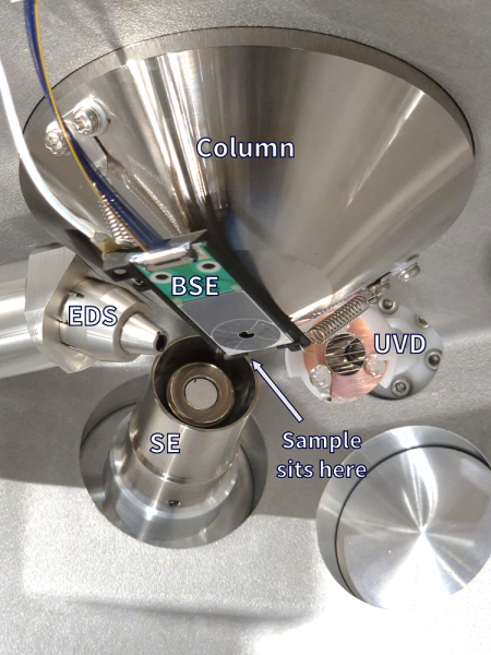
Detectors on the FlexSEM

Detectors

The detectors for the SEM are positioned around and above the sample stage, all generally directed towards the same point in space where the electron beam will be focussed onto the sample. The FlexSEM has the following detectors available for different signals:

SE - secondary electron detector, for topography imaging

BSE - back-scattered electron detector, for material contrast

EDS - energy-dispersive X-ray detector, for elemental identification and quantification

UVD - ultra-variable detector, for use in VP-SEM, and also for cathodoluminescence (CL) imaging

Note how the BSE detector sits directly above the sample, and the electron beam passes through the centre of the four quadrants of this detector.

Next - Electron interactions and detected signals

Back to MCFP Learning Home

Materials Characterisation and Fabrication Platform

  • Our Capabilities
    • Nanofabrication
    • Nanomaterials Characterisation
      • Atomic force microscopy
      • Anton Paar NHT3 Nanoindenter
      • DataPhysics optical contact angle
      • Hirox RH-2000 2D/3D microscope
      • Quorum Q150T Sputter Coater
    • Advanced Fluorescence Imaging
      • Zeiss Elyra 7 Lattice SIM
      • Nikon A1R+ Confocal Microscope (CLSM)
      • STORM (Stochastic optical reconstruction microscopy): Nikon N-STORM
      • Olympus IX71 Fluorescence Microscope
    • Cytometry and Particle Characterisation
      • Mass cytometry
      • Halo
      • NanoSight Pro
      • Apogee A-50 Microflow Cytometer
      • CytoFLEX Nano
      • Imaging Flow Cytometry
      • ICP-MS
      • Imaging ToF-ICP-MS
    • Electron and Ion Microscopy
      • Scanning electron microscopy (SEM)
      • Helium ion microscopy and dual-beam nanofabrication
      • Sample Preparation
    • X-Ray Characterisation
      • X-ray diffraction (XRD)
      • X-ray fluorescence (XRF)
    • Vibrational Spectroscopy
      • Confocal Raman Microspectroscopy
      • Fourier Transform Infrared Microscopy
    • Biological Optical Microscopy Platform (BOMP)
    • Ian Holmes Imaging Centre
    • Trace Analysis for Chemical, Earth and Environmental Sciences (TrACEES)
    • University of Melbourne Research Infrastructure
    • MCFP 2023 User Survey
  • Access Equipment
  • MCFP news and events
    • MCFP Image Competition
      • MCFP Image Competition
  • Our Expertise
    • Elena Taran
    • Anders Barlow
    • Paul Brannon
    • Darryl Johnson
    • Dan Smith
    • Raveen Wijesuriya
    • Tian Zheng
    • Ray Dagastine
    • George Franks
  • Services for Industry
  • MCFP Learning
    • Video Guides
      • LUMOS ATR-FTIR Guides
      • CytoFLEX Guides
      • NanoSight Guides
      • FlexSEM-EDS Guides
    • FlexSEM-EDS FAQs
  • Sustainability
    • Sustainability Framework
    • Sustainability on Campus
    • FEIT Sustainability
    • Green Impact
    • Sustainable ANFF
  • Publications
  • Current Students
  • Library
  • Staff

Acknowledgement of Country

We acknowledge Aboriginal and Torres Strait Islander people as the Traditional Owners of the unceded lands on which we work, learn and live. We pay respect to Elders past, present and future, and acknowledge the importance of Indigenous knowledge in the Academy.

Read about our Indigenous priorities

Site footer

  • About us
  • Careers at Melbourne
  • Safety and respect
  • Newsroom
  • Contact
  • Campus locations

Contact details

Phone 13 MELB (13 6352)
International +61 3 9035 5511

Address
The University of Melbourne
Grattan Street, Parkville
Victoria 3010
Australia

Connect with us

  • Emergency
  • Terms & privacy
  • Accessibility
  • Privacy
  • The University of Melbourne (Australian University): PRV12150
  • CRICOS number: 00116K
  • ABN: 84 002 705 224